
Article 1: The Fall of the King: How Intel's Legendary Manufacturing Machine Broke
In our new series, "The Crucible of Creation" by Michael Apemah

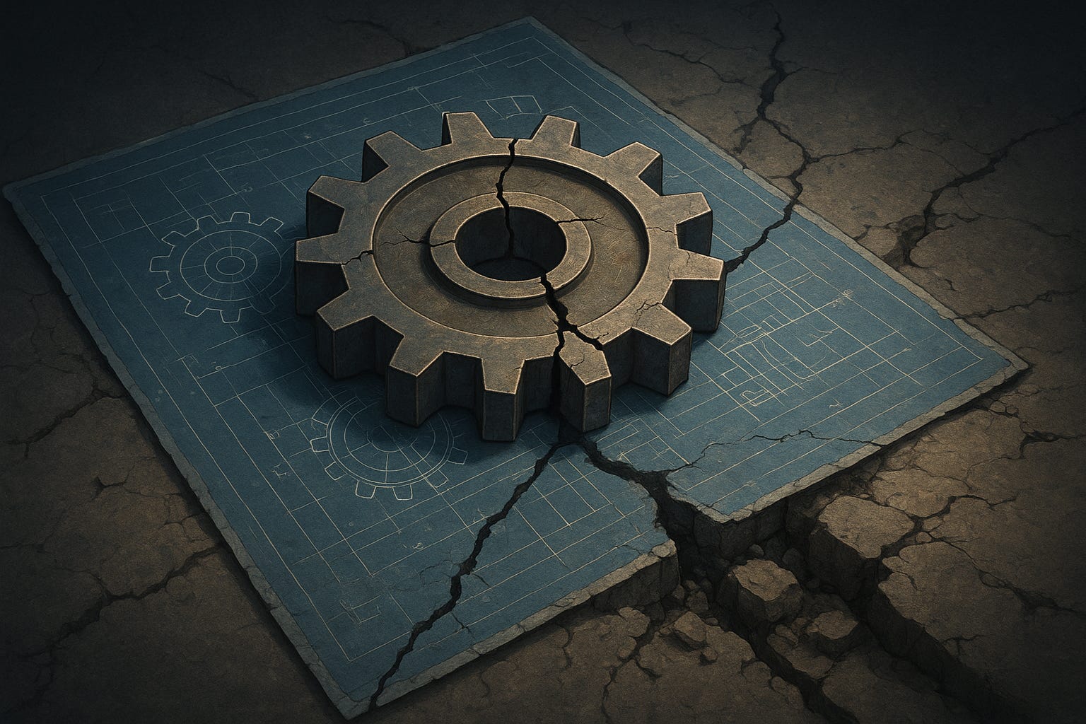
For decades, the semiconductor industry operated under an immutable law of physics: Moore’s Law. And for decades, that law was enforced by a single, dominant power: Intel. To work at Intel in the early 2010s was to be part of a well-oiled machine, an army that marched in a perfect two-year cadence, delivering a new, more powerful manufacturing node like clockwork.
I was a process engineer on the 22nm node. I saw the machine at its peak. It was a thing of beauty and brutal efficiency. But I also had a front-row seat to the very first tremors that preceded the earthquake. The story of how Intel lost its crown is not one of a single, catastrophic failure, but of a slow, creeping sickness—a crisis of physics compounded by a crisis of culture.
What is “Yield”? The Currency of the Kingdom
Before we dive into the crisis, we must understand the single most important metric in a fab: yield.
Imagine you are baking a massive sheet of cookies (a silicon wafer). Your recipe is supposed to make 500 perfect cookies (chips). But when you pull the sheet out of the oven, some cookies are burnt, some are broken, and some are stuck to the pan. You only end up with 400 sellable cookies. Your yield is 80% (400 out of 500).
In a fab, a “good” yield means profit, performance, and leadership. A “bad” yield means catastrophic financial losses and, worse, a loss of trust. For decades, Intel’s mastery of yield was the source of its power. Then, things began to change.
The First Tremor: The Troubles with 14nm
The transition from our highly successful 22nm node to 14nm was the first sign that the ground was unsteady. From my vantage point on the fab floor, the ramp felt different. It was slower, more difficult. The yields for early products like the “Broadwell” CPUs weren’t hitting the aggressive targets we were accustomed to.
This initial stumble led to the infamous “14nm+++” era. Publicly, this was framed as a strength—a testament to how much performance Intel could squeeze from a mature node. The messaging was clever: “At the end of the day, Intel sells products, not process.” And it was true; for a time, our 14nm products were still the best. But internally, this was a defensive crouch. It was a necessary improvisation to cover for the fact that the next stop on the roadmap, 10nm, was in serious trouble.
The Earthquake: The Catastrophe of 10nm
The 10nm node was supposed to be a revolutionary leap. Internally, the reason given for its difficulty was the sheer ambition of the design. We were targeting a density improvement (a 2.7x scaling factor) that was far more aggressive than any previous node jump. Compounding this ambition was a fatal decision: to achieve this without using the new EUV (Extreme Ultraviolet) lithography tools that the rest of the industry, particularly TSMC, was beginning to embrace.
The result was a technical nightmare. The process was incredibly complex, and the yields were abysmal. For years.
This is where the crisis of physics created a crisis of culture. The “Truth and Transparency” that would later become a company mantra was nowhere to be found.
The Messaging: The full extent of the yield issues was a closely guarded secret. For those of us who had transitioned out of the fab into business operations, it was impossible to get a clear picture. The business was still profitable, and the public messaging was always optimistic.
The Deflections: When the press reported that competitors were making breakthroughs, the official line was often a technically correct but misleading dismissal. I recall our then leadership, explaining away an IBM 7nm lab announcement by stating that breakthroughs are not the same as high-volume manufacturing. While true, it completely sidestepped the conversation about our own HVM failures. Leaders, like the famous Sohail Ahmed retired, a clear sign of the depth of the crisis.
The Aftershock: The Stumble at 7nm
Even after the lessons of 10nm, the troubles continued. Mike Mayberry, who took the helm of Technology Development, still couldn’t get the next node, 7nm (later renamed Intel 4), on track, even with the introduction of EUV. He and CTO Murthy Renduchintala, the man hired to bring an “outside-in” perspective, both exited the company in the wake of these new delays.
The core problem, as we would later learn, was a monolithic design philosophy. A single defect mid-process could force engineers to go back to near-scratch. It was an all-or-nothing approach in a world that was becoming far too complex for such gambles.
The king had fallen. The manufacturing machine, once the most reliable and fearsome engine in the world, was broken. The question was no longer about maintaining leadership, but about survival. And that would require a new leader, a new philosophy, and an entirely new way of building chips.
In our next chapter, we will deconstruct the audacious plan to fix it: the “5 nodes in 4 years” crusade and the art of forging a path back to leadership.